Manufacturing Engineering Professor Dr. John Patten Western Michigan University developed a laser-assisted micro-processing technology called "μ-LAM", the method will combine laser with a diamond cutter, and the silicon semiconductor ceramic material is heated and softened, and Cutting processing. According to John Patten, “These materials are usually very brittle. If they are tried to deform or process them, they tend to break easily. By softening these materials, we can increase their flexibility and make them easier to process. The μ-LAM processing unit integrates an infrared fiber laser (wavelength range 1000-1500nm). The laser beam is irradiated onto the workpiece through a single point diamond tool with high optical clarity to heat the workpiece material above 600 °C. Diamond tools with a radius of 5 μm to 5 mm are bonded by epoxy (for milliwatt laser power processing) or by soldering/brazing (for processing of 1 watt or more laser power). Connect to a laser mounted in a tungsten or carbide housing. Other engineers and technicians have tried to process brittle materials (such as ceramics) in a variety of different ways. One method is to first heat the workpiece in the furnace and then process it; the other method is to use laser heating and diamond tool cutting, respectively. The method invented by Patten combines laser and diamond tools, which has significant advantages. He explained, “Things are much simpler, because the laser is aligned with the tool itself, and the laser is heated just at the cutting edge of the tool, so that the best results can be obtained. In addition, the workpiece material is not excessive. Heating.†Patten says μ-LAM processing technology can also cut processing time and processing costs and achieve a very smooth optical surface. “When using conventional machining methods, if you want to make an optical component (such as a mirror), you usually need to start with casting the workpiece blank and then carry out a series of processing steps: rough grinding, fine grinding, grinding, and finally forming. The machining method replaces the original series of processes, cutting with a single-point diamond tool on a CNC machine tool, and also achieving excellent surface roughness (Ra1-10nm).†Patten is working with a Japanese company to achieve Commercial application of the μ-LAM system. He expects the invention to find its place in a number of industries, including automotive, aerospace, medical equipment , semiconductors and optics. “Our initial goal was to target the optical and semiconductor industries, but now it seems that most of its applications will be on high-energy, high-temperature microelectronics . In the semiconductor industry, silicon is the carrier of chips and integrated circuits ,†he said. Silicon carbide is used in higher temperature operating conditions. Therefore, almost all of our energy is now focused on the processing of silicon carbide."
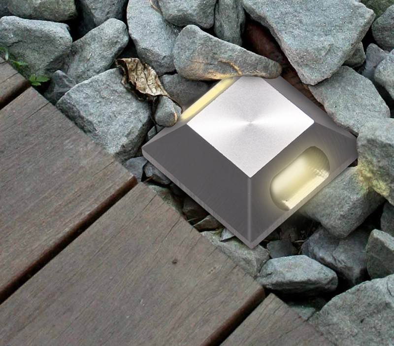
LED Side-emitting LED underground lamp is made of 304 stainless steel, and the surface is treated with electrostatic spray, which is cured at a constant temperature and has strong adhesion. Generally have good waterproof and dustproof properties. The design with different angles of light on the side can better decorate the outdoor landscape.

Our other products range:LED Underground Light, LED Underwater Light , LED Wall Washer Light, LED Linear Light , LED Outdoor Flood Light, LED Garden Light , LED landscape light , LED Strip Light , LED Step Light etc.
Side Emitting Inground Light,One Side Step Light,Recessed Led Light,1W Underwater Light
SHENGYA LIGHTING TECHNOLOGY CO., LTD. , https://www.syalighting.com